● COG Process
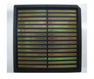 | Chip On Glass(COG) Technology
COG in much of the (chip on glass) wafer ic pad on the ground conductivity are shaping the bump driver ic glass the on the panel ACF film (anisotropic conductive file : Anisotropic conductive file) using Access to advanced bonding As technology, which requires a high resolution large numbers of (contact point / channel) the point of contact and (higher resolution) mobile lcd (liquid crystal display) the product that applied technology. |
| | |
● TAB & Probing Test
TAB(Tape Automated Bonding) & Probing Test
nepes is providing the Full Turnkey Solution of the Display Drive IC package such as Gold bumping, Wafer Probing Test, TAB(Tape Automated Bonding), and Chip Probing Test with back-end process having wafer back-grinding, marking, and dicing saw process.
● Product View

● Process Description
 | Chip On Glass(COG) Technology
COG in much of the (chip on glass) wafer ic pad on the ground conductivity are shaping the bump driver ic glass the on the panel ACF film (anisotropic conductive file : Anisotropic conductive file) using Access to advanced bonding As technology, which requires a high resolution large numbers of (contact point / channel) the point of contact and (higher resolution) mobile lcd (liquid crystal display) the product that applied technology. |
| | |
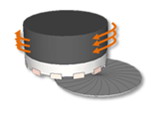
 | Wafer Back-grinding Technology
Wafer back-grinding is a step during which wafer thickness is reduced to allow for stacking and high density packaging of the chip. For smaller and thinner packages for portable and hand-held products, the backside of the wafers are ground prior to wafer dicing. |
| | |
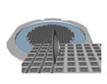
 | Wafer Dicing(Sawing) Technology
In this process, the individual chips(IC) are separated by mechanical sawing. During dicing,�the wafers are mounted on dicing tape which has�a sticky backing that holds the wafer on a thin sheet metal frame. |
| | |
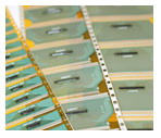
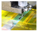 | Inner Lead Bonding(ILB) Technology
On the processes, the chip is placed on external circuitry by attaching the bumps on the chip to the inner lead on polyimide film (COF) to connect electrically |